Czochralski Silicon Crystal Growth and Characterization
K. Daido, S. Shinoyama and N. Inoue
Review of the Electrical Communication Laboratories, "7-1-2, 33-40 (1979).
This paper describes oxidation induced stacking faults (OSF) in dislocation-free Czochralski silicon, formation mechanism and growth technique for low defect density crystals. OSF-free (less than 100/cm2) silicon crystals have been realized by flattening the growth surface and by growth rat fluctuation suppression. Quantitative relationship between OSF-density and precipitated oxygen content in silicon has been clarified. Furthermore, TEM analysis revealed that the stacking faults are nucleated at the silicon oxide precipitates during hat treatments.
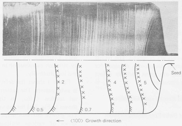
Fig. 1 Swirl pattern s reveled by Dash etch. Annealing condition is at 850 oC for 3 hours in Argon atmosphere.